Introduction
During the 2020 pandemic many of us picked up new hobbies, from making sourdough starter to cycling, etc. As for myself, I started exploring the custom mechanical keyboard scene, something I was interested in prior to the lockdown, yet had not grasped the variety and layers of creative outlet this niche hobby offered. Initially I was exploring designing custom keycaps (think artisans, minus the art). By using my SLA 3D printer, I was particularly curious to mix my design knowledge in Fusion and Rhino to produce prototypes with the the printer and then use traditional resin casting to produce batches. Unfortunately, this project hit a road block due to logistical and cost issues obtaining a resin pressure pot in the UK. However, I was able to produce a few concept keycaps which I plan to do a small write up about soon™.

Back to the topic at hand, recently when watching an episode of Keebcast (Keebcast #33 ft. Wilba) the question of how someone with little EDA knowledge could learn to design a keyboard’s PCB, was asked.
For those unfamiliar with the abbreviation, PCB stands for printed circuit board and most of the technology we use on a day to day bases houses a PCB. In terms of mechanical keyboards, the PCB is housed within a case, often made of injection moulded plastic or cnc’d aluminium. The case often supports both a PCB and a plate, the plate is used to occasionally support the PCB itself and the mechanical switches, which connect to the PCB and act just like any other mechanical switch you can think of such as a light switch.
The proceeding conversation piqued my interest in attempting to design my own PCB for a “simple” 3 switch by 3 switch macropad, which I could use for shortcut keys, macros, etc within much of design software I utilise on a day to day basis.
Firstly, a few housing keeping points! I am an architect working full time, that happens to have an interest in consumer electronics, electronic design, and if you haven’t realized yet, mechanical keyboards. This series could be beneficial in helping others find out where to gain information and assistance in designing their own PCB, however, it is not intended to be a tutorial or guide on how to design a PCB, but rather to document my processes, both success and failure. Therefore, don’t consider what you read or see here as a definitive “how to” and expect there to be some major errors in what follows!
I am not an electrical engineer. I am not a programmer. I am just a hobbiest with a passion, who also studied architecture.
As stated above, this series will document my process of attempting to make a simple macropad entirely from scratch, so to speak. I’m starting with the PCB as this is the most challenging part of the process for myself and the aspect I know the least about. Once I have a working PCB in hand I will move onto designing the case and 3D printing this myself in Formlabs clear resin. Therefore, I have no idea how many parts this series will be, but the plan is to keep things as concise as possible. I won’t be going into major details, such as how the actual PCB works (i.e. what this component does, why a resistor of this ohms, etc). However, I will provide links to all the references and documentation I’ve used, which should help others to achieve the same.
Software
KiCad
My choice of software, KiCad, was informed by both Wilba’s suggestion on Keebcast and ai03’s Guide to Keyboard PCB design. For those not familiar with these names Wilba is the designer of all of Rama Works’ keyboard PCBs and ai03 is a highly regarded keyboard designer.
There are a number of other great reason to use KiCad for your PCB design. It’s open-source and free to use, even for commercial projects, the hobbyist community often uses KiCad and therefore many of the online guides use KiCad. Lastly, the software is surprisingly intuitive and in the last couple of weeks learning it I’ve found that it has very few idiosyncrasies. Anyone with prior CAD experience should not have any difficulty picking it up.
Alternative EDAs
I’ve not explored the wide world of EDA software much outside of KiCad, so rather than list the pros and cons of each. I thought I would simply list a few highly recommended alternatives.
If you’re particularly fond of Autodesk (may god have mercy on you’re soul) there is Eagle. Which is a relatively powerful EDA tool and for those invested in Fusion 360, you may want to consider this option as it’s included in your subscription. To my knowledge Eagle does have a free tier but cannot be used for commercial projects and has a limit of an 80 cm2 board, which is too small even for a macro pad.
To avoid the eagle board size limitation, make a Fusion360 account, download it and then login with that into eagle. The Fusion 360 Free license also comes with an EAGLE subscription with less restrictions that gives you enough room to do any keyboard pcbs.
lastly I will also mention Altium, which is far more professionally focused and almost completely overkill for a small hobby project such as a custom keyboard. With that said Altium is incredibly powerful and supports complex routing options not available in KiCad. However, Altium is also crazy expensive, but does have a student tier.
Resources
Grab this project
I’ve open-sourced this entire project (under a MIT License) as it was mostly made possible by studying other open source resources and I’ve no intention of commercialising this specific project. Furthermore, the project still needs to be tested to confirm the design actual works. Therefore, please remember these KiCad design files are provided as is and no guarantee is made of their accuracy, use at you’re own risk. (i.e. if you use or modify these files and blow you’re PC’s USB port that is not my fault!)
At the time of writing this post, I’m fairly committed to the project and will be pushing regular updates to the GitHub repository. In either Part 2 or 3 of this series we will hopefully have an in hand PCB and be able to test the design.
PCB designed by Jeremy Paton (Rev A Untested)
Project specifications
- 9X 1U MX-Hotswap switches
- USB-C support
- Atmega32u4 support (MU QFN-44 version)
- Per-key RGB LED (9 LEDs)
- RGB Underglow (4 LEDs)
- Over current & reverse bias protection
- ESD protection
- QMK support
- Designed in KiCad 5.1.9
Resources
ai03’s PCB Guide:
I strongly believe the “PCB Designer Guide“ by ai03 is one of the most significant pieces of literature or knowledge that has been produced in the custom keyboard community . This is certainly not to say that it is all encompassing, there are some notable omissions including, incorporating USB-C and daisy chained RGB LEDs. However, for a leading member of the community who has a commercial interest in their knowledge to share such information in an easily digestible format is unique to say the least. This is where I suggest everyone should start learning!
Discord:
Discord in general was a massive help to me in learning and asking odd questions as I slowly worked on the schematic circuit design for my keyboard. The Discord search will be you’re best friend and kicks Google’s but at providing relevant information. With that said what discord servers did I use?
If you join any of these Discord servers, please be nice, and remember the members are volunteering their time and support and no one is entitled to provide any help. Please read their rules and check their FaQ channels!!
Youtube:
Much like Discord, YouTube is a treasure trove of information on PCB design. From tutorials on EDA software to general circuit design principles. However, finding targeted information on designing a keyboard can be al little more challenging. The following videos should help:
- MrKeebs’ – PCB from Scratch with Gondo
- Hadi’s – PCB design series (incomplete ATM)
- KoBuss’ – How we designed a mechanical keyboard PCB
Blogs/Websites:
The following resources were particularly useful on understanding and implementing parts of my design, such as the ESD and reverse bias protection:
Schematic Design
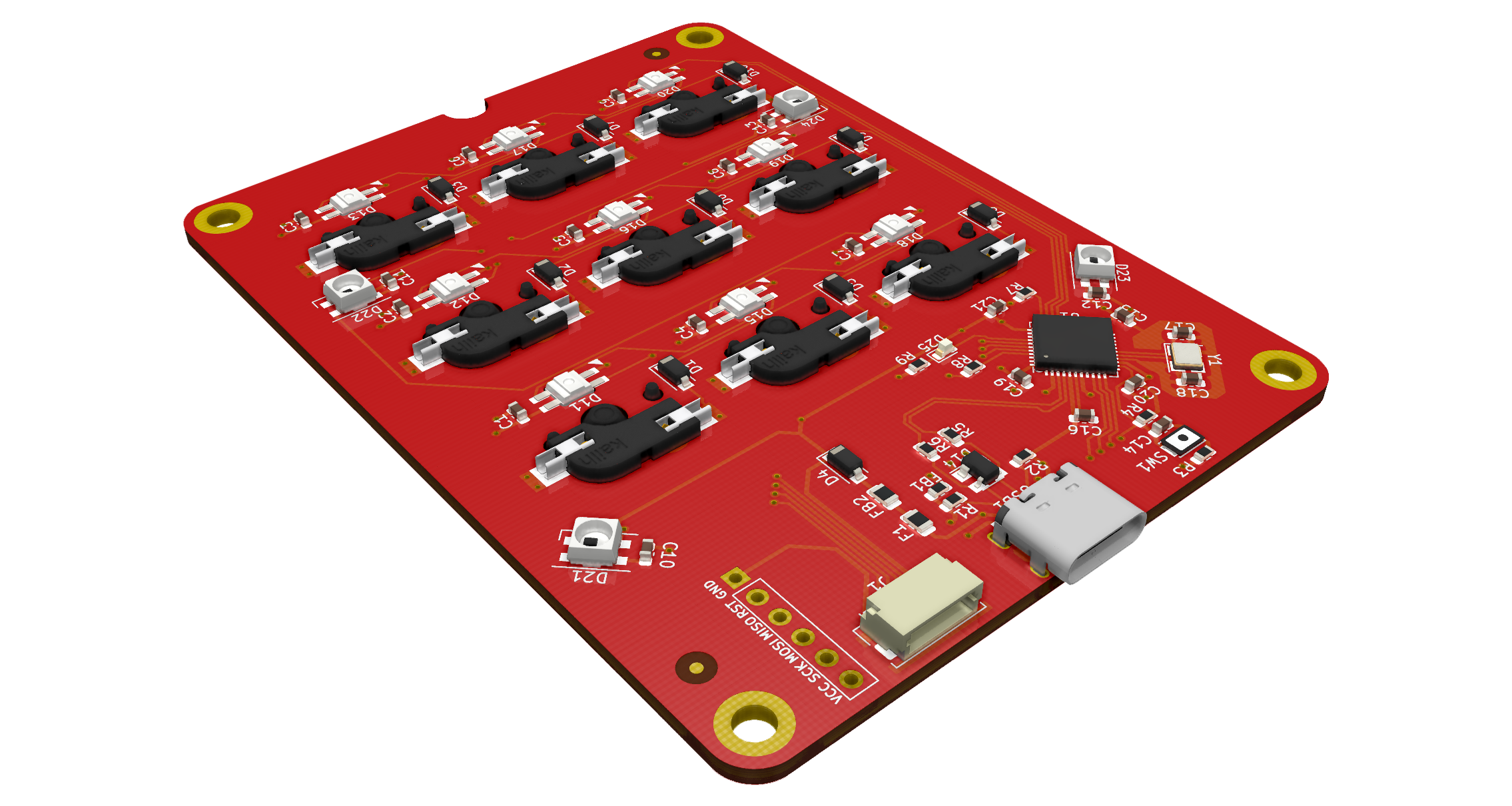
Whilst I connected the dots and defined the specifications of the project, this schematic is the product of the combined efforts of many individuals. Please be aware that at this point it has not been tested but the general implementation is not particularly unique and follows the rules, guides and suggestions given to me along the way.
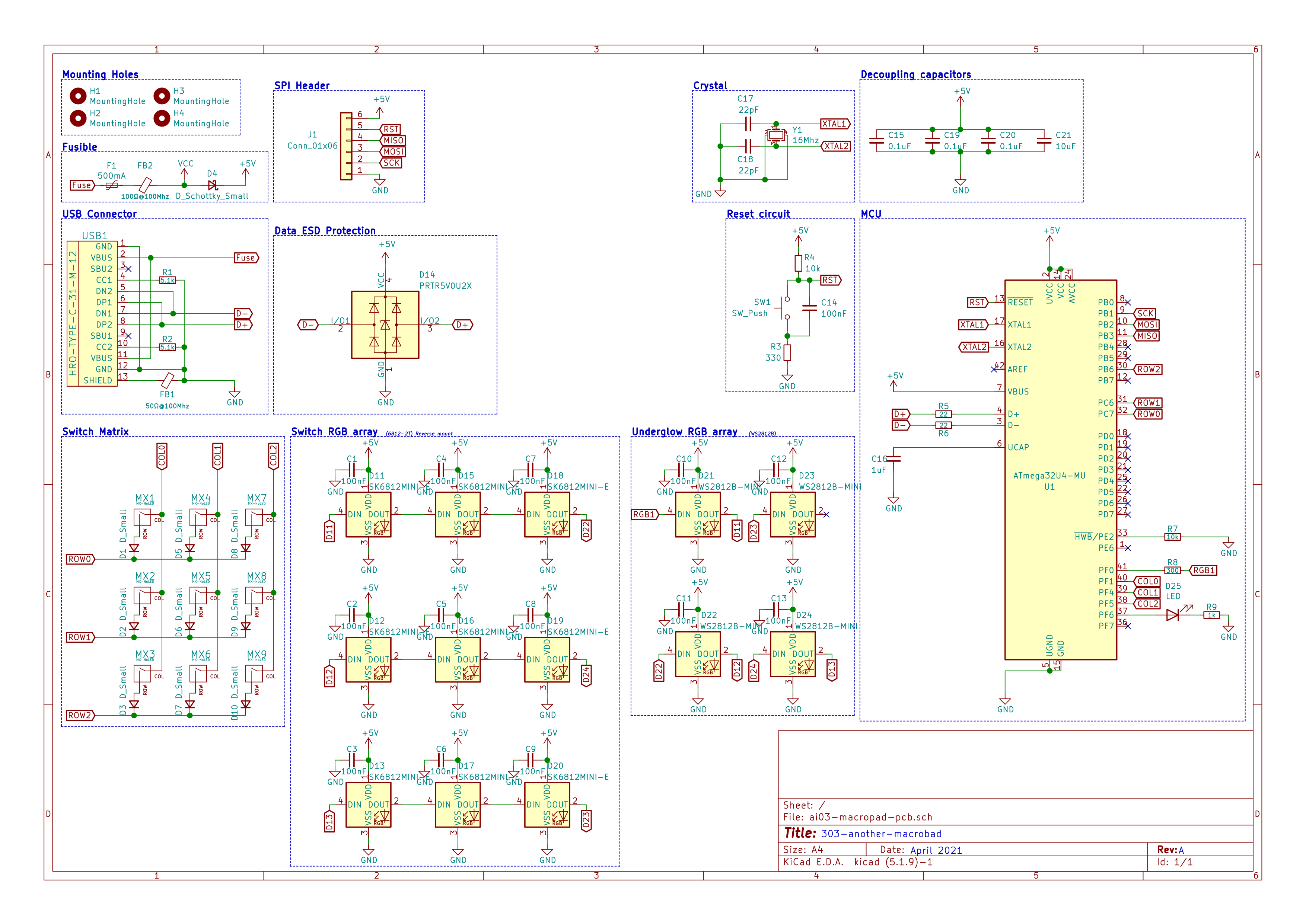
PCB schematic designed in part by myself. UNTESTED!
Whilst I won’t go into extreme detail outlining each component in the above schematic. A few notable unique elements of the design include 9 RGB LEDS for per-key switch lighting. I’ve opted to use the SK6812Mini-E LEDs which are reverse mount and thus will save on assembly cost as all components can be placed on one side of the PCB. There are an additional 4 RGB LEDs, specifically the WS2812B-Mini, for underglow (which may require revision based on the case diffusion once tested).
On RGB LEDs:
The SK6812Mini-E, WS2812B-Mini and WS2812B(-B) whilst different in package (size) and possibly pin layout, they all work electrically the same. (i.e. They are all daisy chained RGB LEDs, yet retain per led control).
Reset circuit:
The particular implementation of the reset circuit is somewhat more involved and was based on the design explained by Gondo within the MrKeebs’ – PCB from Scratch with Gondo series. But could be simplified.
USB-C:
Lastly, and a notable departure from ai03’s guide is the use of a USB C connector. USB-C is actually a bit of a nightmare to support but has been significantly simplified by utilising the TYPE-C-31-M-12 connector which simply implements USB 2.0 over the USB-C connector standard.
Routing
Again I won’t be going into too much detail about the routing and specific placement of components. The basic rules apply that the MX switch footprints need to be placed next to one another. To assist in this the following grid settings are recommended within KiCad, based on ai03’s guide:
Set the user defined grid size to 0.79375mm (19.05/24). This value is just fine enough for placing diodes, and just rough enough for easily placing switches. Set fast switching: grid 1 to user grid (0.79375mm) and grid 2 to 5mil (0.1270mm). This allows fast grid switching by holding Alt+1 and Alt+2. 5mil is a value well suited for routing.
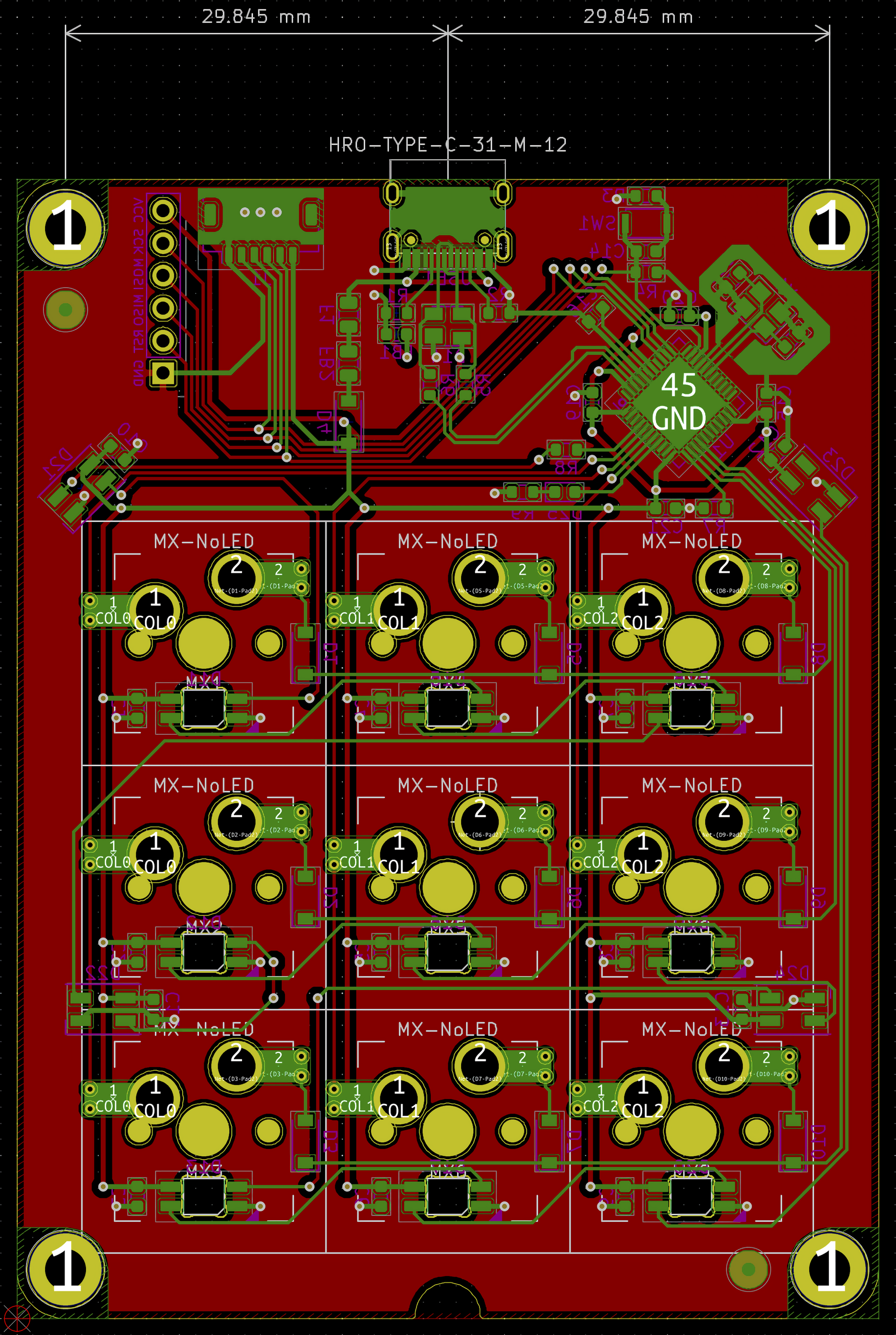
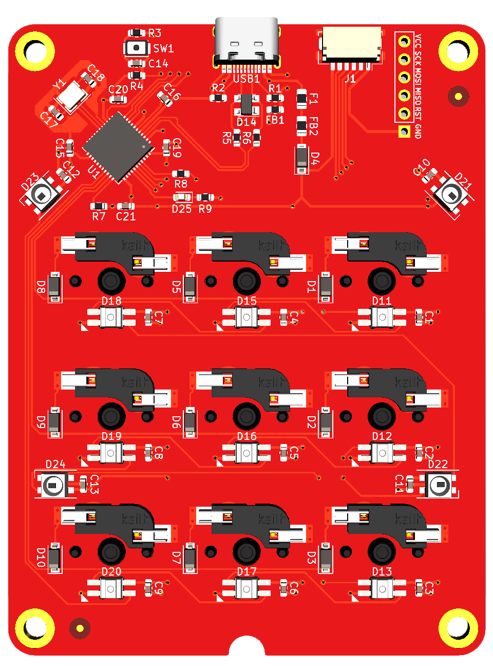
PCB routing with ground plane on back. UNTESTED
A few notable points to make about routing! First keep the USB data lines (D+ and D-) as short as possible by placing the MCU nearby to the USB connector. However, more importantly, run them parallel using the differential pair routing tool to be able to tune their lengths to be equal.
Consider routing horizontal tracks on one side and vertical on the other, the following considerations should also be maintained:
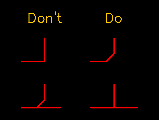
Routing dos and do nots!
I will focus a little bit more on the process of routing and go into a little more detail about the specific implementation of the schematic into the above PCB in part 2.